View All Posts
read
Want to keep up to date with the latest posts and videos? Subscribe to the newsletter
HELP SUPPORT MY WORK: If you're feeling flush then please stop by Patreon Or you can make a one off donation via ko-fi
#CONDUCTIVE INK #FRAGILE BONDING #HIGH COST #HOME ELECTRONICS #PCB MANUFACTURING #PCB PROTOTYPING #VOLTERA

I’ve been given a Voltera machine to do some PCB prototyping at home (thanks Rob!). These are pretty amazing machines.

Voltera V-One including Drill head

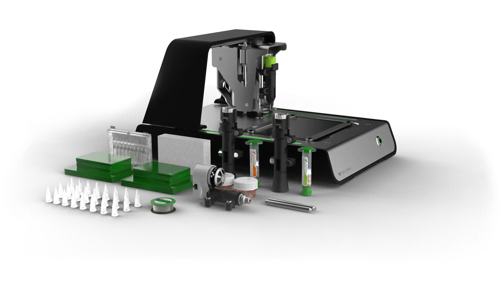
They use conductive silver ink to create the traces and pads. When this works it’s incredible - when it doesn’t, it’s very much like 3D printing with a lot of messing around.

Is it the end of the PCBWay+atomic14 relationship? Well, not really, there are some quite serious limitations.

There is a drill attachment for the machine and you can create vias and the equivalent of plates through holes using small rivets. But I don’t have the drill attachment and I think trying to line up the top and bottom layers would be pretty difficult.

Trace width and spacing is a minimum of 8 mil (0.2mm). For the design I did I went with 4mm to be safe.

There’s a minimum of 0.65mm pin pitch for SMT IC packages and they recommend using a minimum of 0603 passive component size.

The conductive ink bonding to the board is also not very strong, so any components that might get physical abuse can be quite fagile.

You also need to use special low temperature lead free solder paste.

But, the biggest limitation is the price! The machine costs $5000+ US and the ink and paste are both pretty expensive.

End to end the process is pretty quick, with practice you could be producing PCBs in 1-2 hours.

The process is pretty straightforward once you’ve got your PCB designed.

  • Clamp the board in the machine and align the circuit with it
  • Probe the height of the board to build up a height map
  • Prime the conductive ink dispenser and check the calibration
  • Print the circuit
  • Cure the conductive ink
  • Wait for the machine to cool down
  • Prime the solder paste dispenser
  • Dispense the paste
  • Place the components - this is a manual step - no pick and place built in
  • Reflow

All in all it’s a great addition to the workshop for doing quite prototypes, but it’s not going to replace having a proper PCB manufacturer.

#CONDUCTIVE INK #FRAGILE BONDING #HIGH COST #HOME ELECTRONICS #PCB MANUFACTURING #PCB PROTOTYPING #VOLTERA

Related Posts

Making hard pcbs at home - In my latest DIY adventure, I explored nickel plating to harden PCBs at home. I was inspired by a slick resistor box design I found through EEVBlog, which had an incredibly cool switching technique but left the PCBs vulnerable to wear from contact scraping. Despite some initial mix-ups and challenges—like dealing with steel instead of pure nickel, using the wrong voltage, and dealing with contamination—my experiments led to some promising results. I even compared the scratch resistance of plated vs. original PCBs in a very informal test. I wrapped up by sharing some handy links for anyone eager to dive into their own nickel plating escapades. It's clear that more experiments are on the horizon!
Scripting KiCad to make coils - I've been diving deep into the world of PCB (Printed Circuit Board) coils, inspired by Carl Bugeja's incredible PCB motors! After deciding to set up an automated process for creating the coils rather than manually drawing them (can you imagine?), I found our main constraints became track width and spacing, and the number of layers we could use. During the process of creating spirals for our coils, I encountered some interesting problems - spirals are easy, but what about arbitrarily shaped coils? My attempts ultimately lead me to develop more efficient algorithms and KiCad plugins to generate these special coils. A rewarding challenge of math, programming, and electronics! My code has been published on GitHub, and I’m eager to see how others might make use of it!
The PCBs are in production - what have I messed up? - After some stress and trepidation, I finally took the plunge and sent my PCB design off for manufacturing. My design centers around building a large seven-segment clock with LED filaments. Jumping hurdles such as voltages, pin usage, and limiting the load on my power supply, I've settled on the ESP32 as the system's heart and come up with a final circuit design. While doing this, I've quickly realized I could improve my layout and fixed a small mistake. Also, I've prepared for either types of LED filaments - the high-voltage ones or the larger, 3v ones. However, I did bungle up a couple of things on the enable line of the shift registers and board layout. But hey, this is a learning curve, right? Can't wait to get the boards and see what other exciting errors surface!

Related Videos

Printing PCBs At Home! - In today's captivating episode, I take a shot at home printed PCBs rather than buying from our faithful PCBWay, leading to some riveting discoveries. Using a stunning Voltera machine, my single-sided print echoed a glistening marshmallow-like texture that was cured just lovely in the oven. Encountering limitations, such as weak conductive ink bonds and layout tricks, brought on new challenges but also widened my horizon for potential improvements, such as considering a direct USB connection experiment. Despite issues, our creation came to life through intriguing stages of soldering, placement, and reflow, resulting in a successful quick prototype with operational LEDs and programmable features! Our exploration does remind me of the value of PCBWay though so have no fear, our Atomic 14-PCBWay partnership continues on. Keep watching for more such adventures!
Lovely High Res E-Paper Display - Just when we thought we'd done with our mailbag, some exciting new stuff tips up. This time, we've got a soldering kit, a fun-looking Dash, and extra bonus, an ink plate 10, which is a cool e-paper display from Soldered. We've unboxed it, pulling out a board with an esp32 module, an SD card, and a battery connector. One of the major selling points is its open-source nature, you can download all the schematics from GitHub, and for those inclined, learn about how to build pcbs. Also showcased a Simon Says game soldering kit, despite my modest soldering skills (we all need practice, eh?), it turned out to be good fun. Plus, we've got a Dev board fitted with an at Mega 328p and an ultra-bright ws2812 RGB LED. Let's see if I can turn this e-paper display into a weather display or maybe you have more exciting ideas, drop them down in the comments!
How Good Are My USB Cables? - In this video, I engage in a deeper exploration of USB testing, encountering a range of trials and tribulations along the way. First up, I attempt to test a couple of USB cables and discuss their data lines' peculiar situatedness. Then, I delve into the assembly of the PCB boards, sourced from PCBWay, which surely turned into a learning voyage than an easy sail. The first version faced challenges of misordered large-frame stencil, unseen connection problems, and even DRC errors in the submission process. Not dwell on that, I redesign and bring to table Version 2, complete with USB connectors with broken-out pins and designed for visual inspection ease. Although this version demonstrated success, soldering difficulties and bad connections persisted. Considering all the hurdles, I decide to let PCBWay handle the assembly for the next version. For future strategies, adding test points and eliminating the lithium-ion charging circuit seemed more practically viable. Peeping into version 3, testing points for all USB cable pins have been added and even an option to break out actual USB connections, all towards ensuring an improved error checking and usefulness of the assembly.
PCB Mistake Turns into Vacuum Stencil Experiment | MHP30 Hotplate Test - Learn how to recover from a mistaken chip order and improve SMD soldering techniques using a mini hotplate and vacuum cleaner stencil holder. Watch the mesmerizing results under the microscope!
Nickel Coating PCBs At Home - In this experiment-filled video, I explore the inner workings of a resistor box I spotted on the EEVBlog channel. With its ability to adjust in increments down to 0.1 ohms, I was fascinated, but also noticed the binding posts could do with an upgrade. Upon inspection, I was intrigued by the simple yet clever construction and the possibility of enhancing the durability of the copper with some nickel plating. Navigating through the potential challenge of the resistors on the PCB, I embark on the journey of creating a homemade nickel plating solution. A few hiccups, adjustments, and an hour later, we end up with a liquid emerald green solution, ready for some plating experiments.
HELP SUPPORT MY WORK: If you're feeling flush then please stop by Patreon Or you can make a one off donation via ko-fi
Want to keep up to date with the latest posts and videos? Subscribe to the newsletter
Blog Logo

Chris Greening


Published

> Image

atomic14

A collection of slightly mad projects, instructive/educational videos, and generally interesting stuff. Building projects around the Arduino and ESP32 platforms - we'll be exploring AI, Computer Vision, Audio, 3D Printing - it may get a bit eclectic...

View All Posts