I keep needing the same thing - a really basic dev board for whatever Espressif module I’m playing with. USB-C, a 3.3V regulator, BOOT and EN buttons, three LEDs (5V present, 3.3V present, and one on a GPIO so you can run the blink sketch), and every GPIO broken out on headers. Nothing clever, just the minimum board that gets a bare module doing something.
While building the ESP32 module database I noticed there are twelve modules that fit one sensible recipe - a PCB antenna and native USB - spread across the S2, S3, C3, C5, C6 and H2 families. Native USB is the bit that keeps the component count down. There’s no USB to UART bridge to buy and route, just a USB-C socket and a couple of 5.1K resistors on the CC pins so the host actually hands over power.
Twelve near-identical boards is exactly the kind of job that makes you question your life choices in KiCad.
So I did what everyone on the internet is currently telling you to do and asked Claude to spin up a team of AI agents to design the boards for me.
And it said no.
Not a flat no, more of a “this is beneath me” no. Its argument, roughly - this is a mechanical, repetitive job, and you don’t want a swarm of agents improvising twelve layouts. What you want is deterministic scripts that produce the same board every time, with AI involved only where there’s a real judgement call to make.
Which is a surprisingly sensible thing for it to say. So I let it write the scripts instead, and the AI’s contribution to each board shrank down to a single file. More on that below.
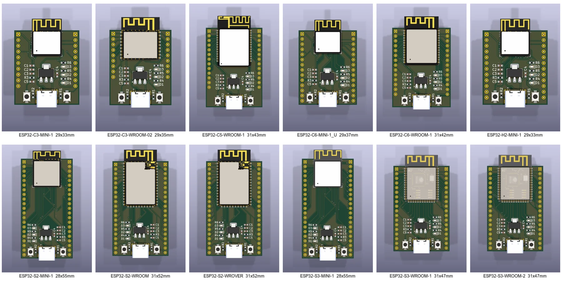
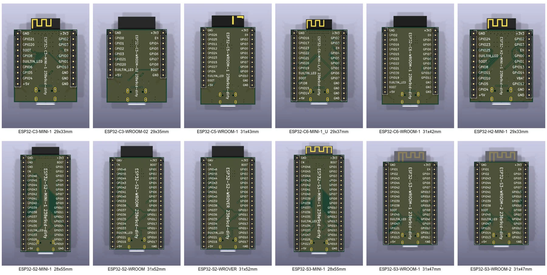
That montage is to scale - the render pipeline normalises the zoom so a 29×33 mm C3-MINI board looks properly tiny next to a 28×55 mm S2-MINI.
The whole thing is on GitHub at atomic14/kicad-esp32-dev-boards, with fab-ready Gerbers and openable KiCad projects for all twelve boards on the releases page.
So what’s left for a human to do?
Almost all of the pipeline is just deterministic scripting. The only real
judgement call is a small board.yaml per module, and it holds the things a
script can’t work out for itself from the symbol and footprint:
- Which pins must not be broken out. This is sneakier than it sounds, because
it’s symbol specific rather than name based -
SPIIO6,SPIIO7andSPIDQSare reserved for the octal flash on an S3-WROOM-1, but the same names are perfectly usable GPIO on the quad S3-MINI-1. - The boot-strap pin that the BOOT button pulls low. GPIO0 on the Xtensa parts, GPIO9 on most of the RISC-V parts, and GPIO28 on the C5, because nothing is ever completely consistent…
- The strapping and input only pins to steer the on-board LED away from. Given that list the generator picks the LED pin itself - the safe pad physically nearest the LED on the laid out board, so the trace stays nice and short. Hang the LED off an input only pin and it simply never lights up, so the build hard-errors rather than let that ship.
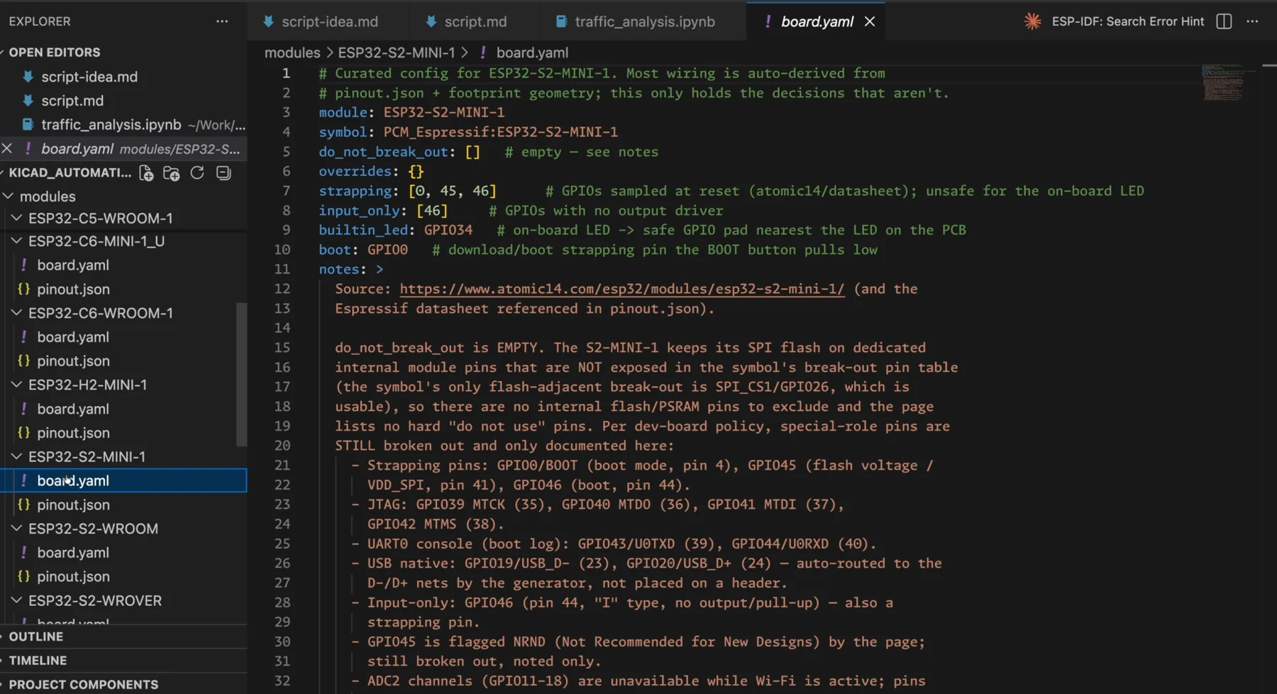
That’s the whole hand written input for a board. Everything else gets derived from the module’s symbol and footprint - power, GND, EN, the USB D+/D- pair, the GPIO net labels.
And this file is where the AI actually lives. All those judgement calls are already written up in plain English on each module’s page of the module database - for humans. So the job I hand to the AI is a simple one: read the page, fill in the file. Messy prose in, clean data out, which is the one thing a script can’t do.
It works under a safety net too. If it picks an unsafe pin for the LED then the build hard-errors and refuses to generate the board at all.
So how does the generator work?
Each board starts from a pre-built skeleton project - the USB-C connector, LDO, buttons and LEDs, already placed, routed and sanity checked.
There are actually two skeletons, mirror images of each other, one with EN on the left and BOOT on the right and one the other way round. That one came out of playing about with the AI. Depending on which edge a module’s reset pin comes out on, putting the matching button on that side makes the routing much easier, so the generator has a look at the footprint and picks whichever skeleton fits.
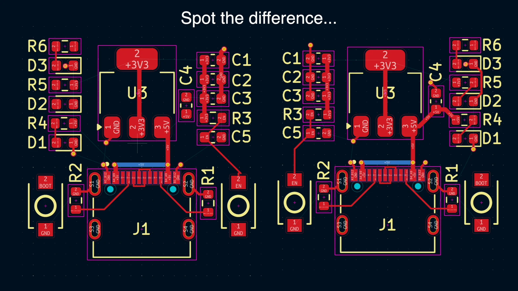
From there the script does four things:
- Builds the schematic with kicad-skip, dropping in the module symbol and two break-out headers, wired up with net labels.
- Places the PCB. USB-C at the bottom edge with the buttons either side of it, support components above that, and the module at the top with the antenna hanging over the edge, as the datasheets demand. The two headers run up the left and right sides, split by a perimeter walk of the module’s physical pin edges, so every GPIO lands on the nearest accessible header pin instead of dragging a track right across the board.
- Autoroutes with KiCadRoutingTools (I run a small fork that keeps vias out of same-net pads). USB D+/D- goes down as a proper coupled differential pair, 0.3 mm centre to centre for 92 to 96% of the run on every board. Every signal is 0.15 mm/0.15 mm, power traces are a wide 0.4 mm, and the whole lot sits under a GND pour with stitching vias. Two layers only, because two layer boards are the cheap ones. All twelve come out fully connected and DRC clean.
- Exports the 3D renders (including the to-scale montages in this post), a validation PDF, and a flat-zipped Gerber+drill package ready to upload to JLCPCB or PCBWay.
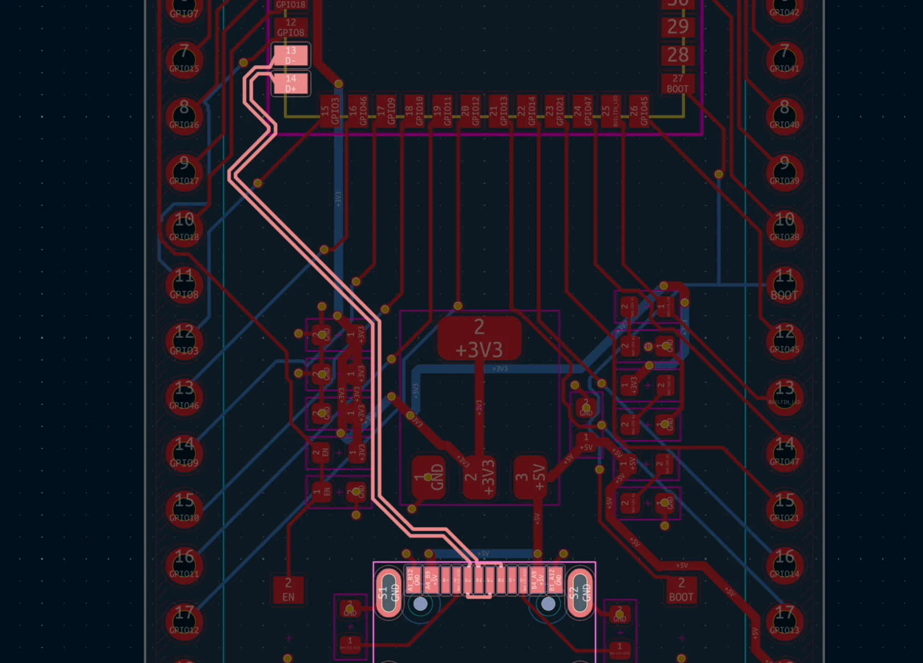
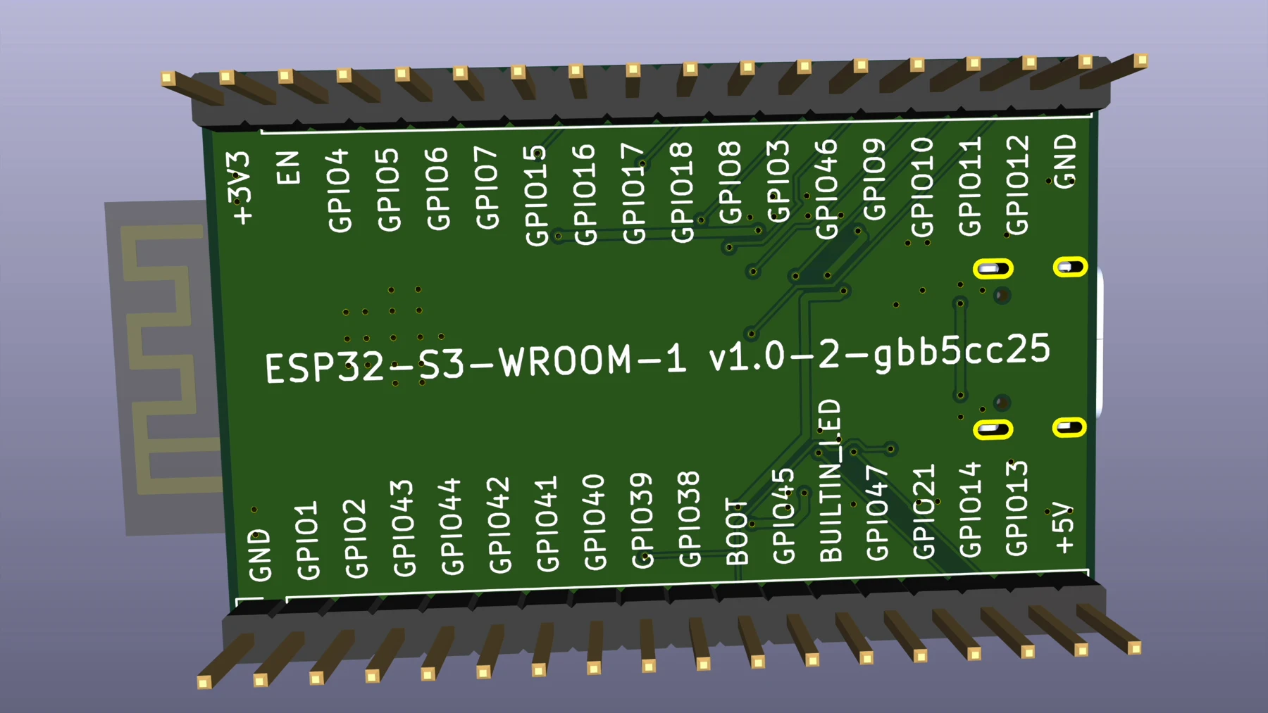
The back of each board gets the pin names in silk next to the headers, and one
little touch I’m quite pleased with - a vertical identifier down the middle
with the module name and the git revision that generated it. That’s just
git describe baked into the silkscreen. Tag the repo v1.0 and every board
fabbed from that tag says so.
Getting it all to run in CI
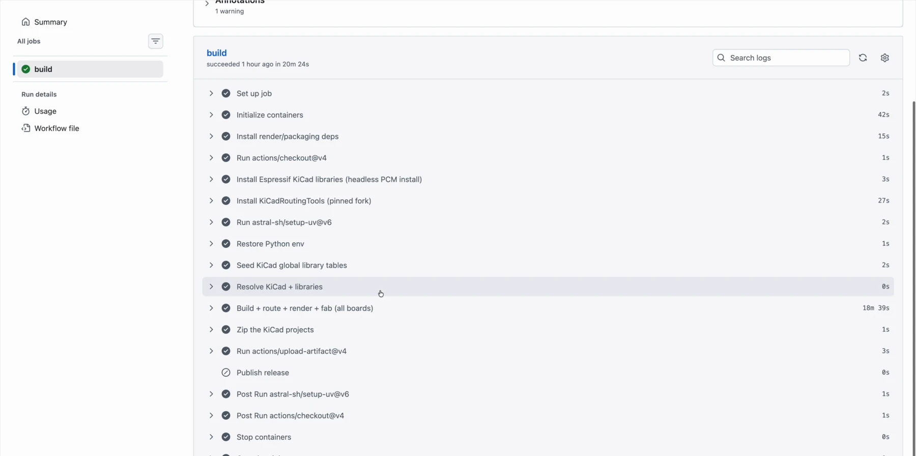
Every push builds all twelve boards on GitHub Actions, and pushing a version
tag publishes a release with the Gerber zips, KiCad projects and montage
renders attached. It all runs inside KiCad’s official Docker image, which is
the supported way to run kicad-cli headless.
Even then, three things bit me. They might save you an afternoon.
kicad-clisegfaulted on startup - even forkicad-cli version. It turned out to be crashing while it scanned the Plugin & Content Manager addon directory, where the Espressif libraries live, when the global library tables don’t exist yet. Which is true on any machine where the KiCad GUI has never been run. The fix is to seed emptysym-lib-tableandfp-lib-tablefiles first.- The zone fills silently didn’t happen. The GND pour is filled by a pcbnew
Python script, and “python3” inside a
uvenvironment resolves to the venv interpreter, which has nopcbnewmodule. Every board came out “routed” but with an empty ground plane and a pile of DRC errors. The fix is to use the python that lives next tokicad-cli. git describerefused to run at all, throwing git’s “dubious ownership” error, because the Actions workspace is bind mounted into the container under a different uid. The boards built fine, but the version stamp quietly fell back to just the module name. Onegit config --global --add safe.directorysorts it out, and there’s now a canary step so it can never fail quietly again.
Getting the boards - but do your own checks
The Gerber zips and full KiCad projects for all twelve boards are on the releases page, ready to upload to your board house of choice.
One honest caveat before you spend any money - these boards are machine generated. They pass DRC with zero errors, they add no new ERC errors against the skeleton, and I do eyeball every render, but I haven’t yet had physical copies of all twelve back from a fab and tested them.
So treat them like any open source hardware design - trust, but verify. Open the KiCad project, sanity check the schematic against the module’s page, and have a proper look at the board before you order. Which is good practice for any design you download off the internet, very much including mine…
I am going to get a batch of these made up, so let me know in the comments which ones you’d like to see. And if you do build one, I’d genuinely love to hear how it goes. If you find a problem, file an issue on the repo so the fix lands in the generator rather than just on one board.
Picking a module for your own project? I've built an interactive ESP32 reference with specs and pinouts for every Espressif module: browse the module database, or compare them all in one big table.